Designing PCBs with Unique Board Edges

Justin Sinichko, Former Hardware Developer
Article Categories:
Posted on
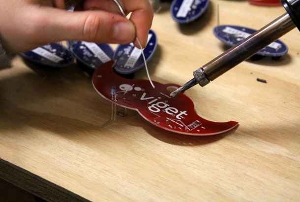
This holiday season we continued one of our cherished holiday traditions -- homemade company vige-gifts. It’s a project on scale with a mini kickstarter and requires time from nearly every lab. This year we made twinkling ornaments, and a custom printed circuit board (PCB) was the centerpiece.

Customizing the shape of PCBs can be difficult. In this post I'll share the tips and tricks we used to punch up our holiday PCB with a custom shape and graphic using Adobe Illustrator, Fusion 360, and Eagle.
Constraints:
PCBs have very specific size and shape constraints. Usually PCBs will need to fit inside something, and often this something will be designed in CAD. We start by working out those size constraints in CAD, then export those constraints in a design-friendly format.
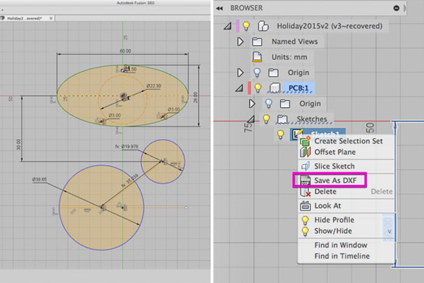
In this example we are using Fusion 360 and we’ve loaded a sketch of our holiday project PCB. There are two primary constraints: a battery holder and the floating Viget logo (3D printed orbs). Notice the sketch guidelines which represent the coin cell battery and orbs. To make this sketch useful we’ll export it as a DXF by right clicking on the sketch and selecting “Save As DXF”.
Use Adobe Illustrator to prepare the DXF file for Eagle. Eagle is our electronic design automation (EDA) software. Import to Illustrator with the following settings:
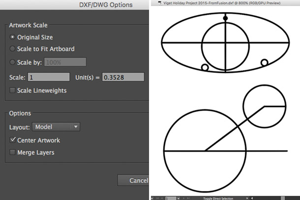
Our CAD model was based in millimeters. Adjust to the units you are working in.
Creating a board edge:
Now we’re in business. Clean up by removing unused shapes and guidelines that were helpful in CAD but are now no longer needed. What is left is a representation of the PCB edge and other important component placement markers. At this point you can modify the PCB edge while being mindful of any constraints.
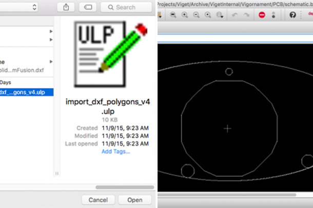
Here is a ULP script that translates a .DXF shape into a PCB edge within Eagle. Thanks Todbot!
Before exporting to Eagle we need to add additional anchor points to the vectors. Our script will essentially draw straight lines between anchor points. So, we want to add as many anchor points as necessary to make the curved lines appear straight.
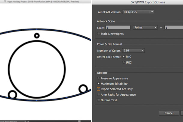
When ready, export a .DXF file from Illustrator with the above settings.
Run this ULP script from within Eagle. First select the script, then the DXF file. When a dialog box appears you should select the layer you wish to draw on -- typically the mechanical layer.
Creating custom PCB graphics:
We want to punch up the visuals on the PCB. We already have an Illustrator file to work with that represents the edges of our PCB. Now all we need is a design. Here were some of the concepts we considered:

We went with a mashup of the above options. To import this to our EDA utility we removed the PCB outline (this isn’t part of the design) and converted the image to a high resolution black and white PNG. Black represents the shape of the silkscreen stencil. A PCB manufacturer will let you choose the ink color. We went with white.

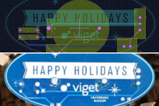
Left: Design comp. Right: Image used by EDA utility.
This was the design we sent to the manufacture and the PCB they shipped us. Huzzah.
We went for simplicity but it could have been a mustache.